- 您现在的位置:买卖IC网 > Sheet目录1214 > EVAL-ADE7880EBZ (Analog Devices Inc)BOARD EVAL FOR ADE7880
�� �
�
�ADE7880�
�The� recommended� procedure� to� manage� SAG� events� is� the�
�IPPHASE/VPPHASE� BITS�
�Data� Sheet�
�following:�
�31�
�27� 26� 25� 24� 23�
�0�
�1.�
�Enable� SAG� interrupts� in� the� MASK1� register� by� setting�
�Bit� 16� (SAG)� to� 1.�
�00000�
�PEAK� DETECTED�
�ON� PHASE� C�
�24-BIT� UNSIGNED� NUMBER�
�PEAK� DETECTED�
�ON� PHASE� A�
�2.�
�3.�
�4.�
�5.�
�When� a� SAG� event� happens,� the� IRQ1� interrupt� pin� goes�
�low� and� Bit� 16� (SAG)� in� the� STATUS1� is� set� to� 1.�
�The� STATUS1� register� is� read� with� Bit� 16� (SAG)� set� to� 1.�
�The� PHSTATUS� register� is� read,� identifying� on� which�
�phase� or� phases� a� SAG� event� happened.�
�The� STATUS1� register� is� written� with� Bit� 16� (SAG)� set� to� 1.�
�Immediately,� the� SAG� bit� is� erased.�
�PEAK� DETECTED�
�ON� PHASE� B�
�Figure� 58.� Composition� of� IPEAK[31:0]� and� VPEAK[31:0]� Registers�
�PEAK� VALUE� WRITTEN� INTO�
�IPEAK� AT� THE� END� OF� FIRST�
�PEAKCYC� PERIOD�
�END� OF� FIRST�
�PEAKCYC� =� 16� PERIOD�
�SAG� Level� Set�
�The� content� of� the� SAGLVL[23:0]� SAG� level� register� is� compared�
�to� the� absolute� value� of� the� output� from� HPF.� Writing� 5,928,256�
�(0x5A7540)� to� the� SAGLVL� register,� puts� the� SAG� detection�
�level� at� full� scale� (see� the� Voltage� Channel� ADC� section),� thus;�
�PHASE� A�
�CURRENT�
�END� OF� SECOND�
�PEAKCYC� =� 16� PERIOD�
�the� SAG� event� is� triggered� continuously.� Writing� 0x00� or� 0x01�
�puts� the� SAG� detection� level� at� 0,� therefore,� the� SAG� event� is�
�never� triggered.�
�BIT� 24�
�OF� IPEAK�
�BIT� 24� OF� IPEAK�
�CLEARED� TO� 0� AT�
�THE� END� OF� SECOND�
�PEAKCYC� PERIOD�
�31�
�0000� 0000�
�24� 23�
�24-BIT� NUMBER�
�0�
�Figure� 57.� SAGLVL� Register� Transmitted� as� a� 32-Bit� Word�
�As� stated� in� the� Current� Waveform� Gain� Registers� section,� the�
�serial� ports� of� the� ADE7880� work� on� 32-,� 16-,� or� 8-bit� words.�
�PHASE� B�
�CURRENT�
�The� SAGLVL� register� is� accessed� as� a� 32-bit� register� with� eight�
�MSBs� padded� with� 0s.� See� Figure� 57� for� details.�
�Peak� Detection�
�BIT� 25�
�OF� IPEAK�
�PEAK� VALUE� WRITTEN� INTO�
�IPEAK� AT� THE� END� OF�
�SECOND� PEAKCYC� PERIOD�
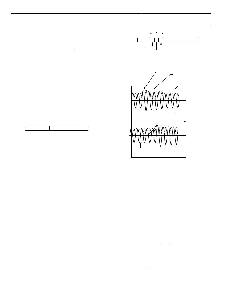
�Figure� 59.� Peak� Level� Detection�
�BIT� 25� OF� IPEAK�
�SET� TO� 1� AT� THE�
�END� OF� SECOND�
�PEAKCYC� PERIOD�
�The� ADE7880� records� the� maximum� absolute� values� reached� by�
�the� voltage� and� current� channels� over� a� certain� number� of� half-�
�line� cycles� and� stores� them� into� the� less� significant� 24� bits� of� the�
�VPEAK� and� IPEAK� 32-bit� registers.�
�The� PEAKCYC� register� contains� the� number� of� half-line� cycles�
�used� as� a� time� base� for� the� measurement.� The� circuit� uses� the�
�zero-crossing� points� identified� by� the� zero-crossing� detection�
�circuit.� Bits[4:2]� (PEAKSEL[2:0])� in� the� MMODE� register� select�
�the� phases� upon� which� the� peak� measurement� is� performed.� Bit� 2�
�selects� Phase� A,� Bit� 3� selects� Phase� B,� and� Bit� 4� selects� Phase� C.�
�Selecting� more� than� one� phase� to� monitor� the� peak� values�
�decreases� proportionally� the� measurement� period� indicated� in�
�the� PEAKCYC� register� because� zero� crossings� from� more�
�phases� are� involved� in� the� process.� When� a� new� peak� value� is�
�determined,� one� of� Bits[26:24]� (IPPHASE[2:0]� or� VPPHASE[2:0])�
�in� the� IPEAK� and� VPEAK� registers� is� set� to� 1,� identifying� the�
�phase� that� triggered� the� peak� detection� event.� For� example,� if� a�
�peak� value� has� been� identified� on� Phase� A� current,� Bit� 24�
�(IPPHASE[0])� in� the� IPEAK� register� is� set� to� 1.� If� next� time� a�
�new� peak� value� is� measured� on� Phase� B,� Bit� 24� (IPPHASE[0])�
�of� the� IPEAK� register� is� cleared� to� 0,� and� Bit� 25� (IPPHASE[1])�
�of� the� IPEAK� register� is� set� to� 1.� Figure� 58� shows� the�
�composition� of� the� IPEAK� and� VPEAK� registers.�
��current� channel� when� measurements� on� Phase� A� and� Phase� B� are�
�enabled� (Bit� PEAKSEL[2:0]� in� the� MMODE� register� are� 011).�
�PEAKCYC� is� set� to� 16,� meaning� that� the� peak� measurement�
�cycle� is� four� line� periods.� The� maximum� absolute� value� of� Phase� A�
�is� the� greatest� during� the� first� four� line� periods� (PEAKCYC� =� 16),�
�so� the� maximum� absolute� value� is� written� into� the� less� signifi-�
�cant� 24� bits� of� the� IPEAK� register,� and� Bit� 24� (IPPHASE[0])� of�
�the� IPEAK� register� is� set� to� 1� at� the� end� of� the� period.� This� bit�
�remains� at� 1� for� the� duration� of� the� second� PEAKCYC� period� of�
�four� line� cycles.� The� maximum� absolute� value� of� Phase� B� is� the�
�greatest� during� the� second� PEAKCYC� period;� therefore,� the�
�maximum� absolute� value� is� written� into� the� less� significant�
�24� bits� of� the� IPEAK� register,� and� Bit� 25� (IPPHASE[1])� in� the�
�IPEAK� register� is� set� to� 1� at� the� end� of� the� period.�
�At� the� end� of� the� peak� detection� period� in� the� current� channel,�
�Bit� 23� (PKI)� in� the� STATUS1� register� is� set� to� 1.� If� Bit� 23� (PKI)�
�in� the� MASK1� register� is� set,� the� IRQ1� interrupt� pin� is� driven� low�
�at� the� end� of� the� PEAKCYC� period,� and� Status� Bit� 23� (PKI)� in�
�the� STATUS1� register� is� set� to� 1.� In� a� similar� way,� at� the� end� of�
�the� peak� detection� period� in� the� voltage� channel,� Bit� 24� (PKV)� in�
�the� STATUS1� register� is� set� to� 1.� If� Bit� 24� (PKV)� in� the� MASK1�
�register� is� set,� the� IRQ1� interrupt� pin� is� driven� low� at� the� end� of�
�PEAKCYC� period� and� Status� Bit� 24� (PKV)� in� the� STATUS1�
�Rev.� A� |� Page� 34� of� 104�
�发布紧急采购,3分钟左右您将得到回复。
相关PDF资料
EVAL-ADE7953EBZ
BOARD EVAL FOR ADE7953
EVAL-ADF4002EBZ1
BOARD EVAL FOR ADF4002
EVAL-ADG788EBZ
BOARD EVALUATION FOR ADG788
EVAL-ADM1021AEB
BOARD EVAL FOR ADM1021
EVAL-ADM1023EB
BOARD EVAL FOR ADM1023
EVAL-ADM1031EB
BOARD EVAL FOR ADM1031
EVAL-ADM1062TQEBZ
BOARD EVALUATION FOR ADM1062TQ
EVAL-ADM1075CEBZ
BOARD EVAL FOR ADM1075
相关代理商/技术参数
EVAL-ADE7880EBZ
制造商:Analog Devices 功能描述:ADE7880, ENERGY METER, 3 PH, SPI, I2C, E
EVAL-ADE7913EBZ
制造商:AD 制造商全称:Analog Devices 功能描述:3-Channel, Isolated, Sigma-Delta ADC with SPI
EVAL-ADE7953EBZ
功能描述:BOARD EVAL FOR ADE7953 RoHS:是 类别:编程器,开发系统 >> 评估演示板和套件 系列:- 标准包装:1 系列:PSoC® 主要目的:电源管理,热管理 嵌入式:- 已用 IC / 零件:- 主要属性:- 次要属性:- 已供物品:板,CD,电源
EVAL-ADF4001EBZ2
制造商:Analog Devices 功能描述:Evaluation Board For Pll Frequency Synthesizer 制造商:Analog Devices 功能描述:ADF4001 PLL SYNTHESIZER EVAL BOARD
EVAL-ADF4002EB1
制造商:Analog Devices 功能描述:EVAL BOARD - Bulk
EVAL-ADF4002EBZ1
功能描述:BOARD EVAL FOR ADF4002 RoHS:是 类别:编程器,开发系统 >> 评估演示板和套件 系列:- 产品培训模块:Obsolescence Mitigation Program 标准包装:1 系列:- 主要目的:电源管理,电池充电器 嵌入式:否 已用 IC / 零件:MAX8903A 主要属性:1 芯锂离子电池 次要属性:状态 LED 已供物品:板
EVAL-ADF4007EBZ1
功能描述:BOARD EVALUATION FOR ADF4007EB1 RoHS:是 类别:编程器,开发系统 >> 评估演示板和套件 系列:- 标准包装:1 系列:PSoC® 主要目的:电源管理,热管理 嵌入式:- 已用 IC / 零件:- 主要属性:- 次要属性:- 已供物品:板,CD,电源
EVAL-ADF4106EB1
制造商:Analog Devices 功能描述:PLL, Frequency Synthesizer